Ideal simulations confirming the fundamentals of the proposed architecture,
component values, power budget, and charge balance.
Architecture
The battery charges a storage capacitor through a 5-stage Dickson charge pump,
boosting 3.1V to 16V. An H-bridge switches the current direction for biphasic stimulation,
while a programmable current sink sets the amplitude from 10 µA to 5 mA.
The MCU controls timing, amplitude, and monitors the system via ADC feedback.
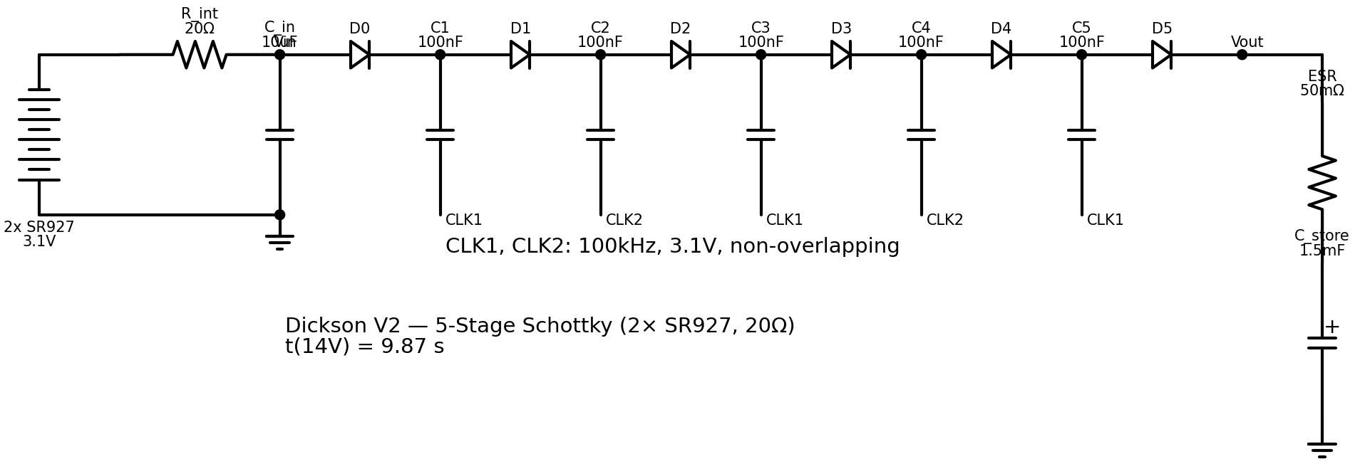
Dickson Charge Pump
5-Stage Schottky Charge Pump
Boosts 3.1V battery to 16V using five flying capacitor stages with Schottky diodes.
No inductor — inherent current limiting protects the SR927 battery.
Clock frequency is firmware-configurable (1–100 kHz).
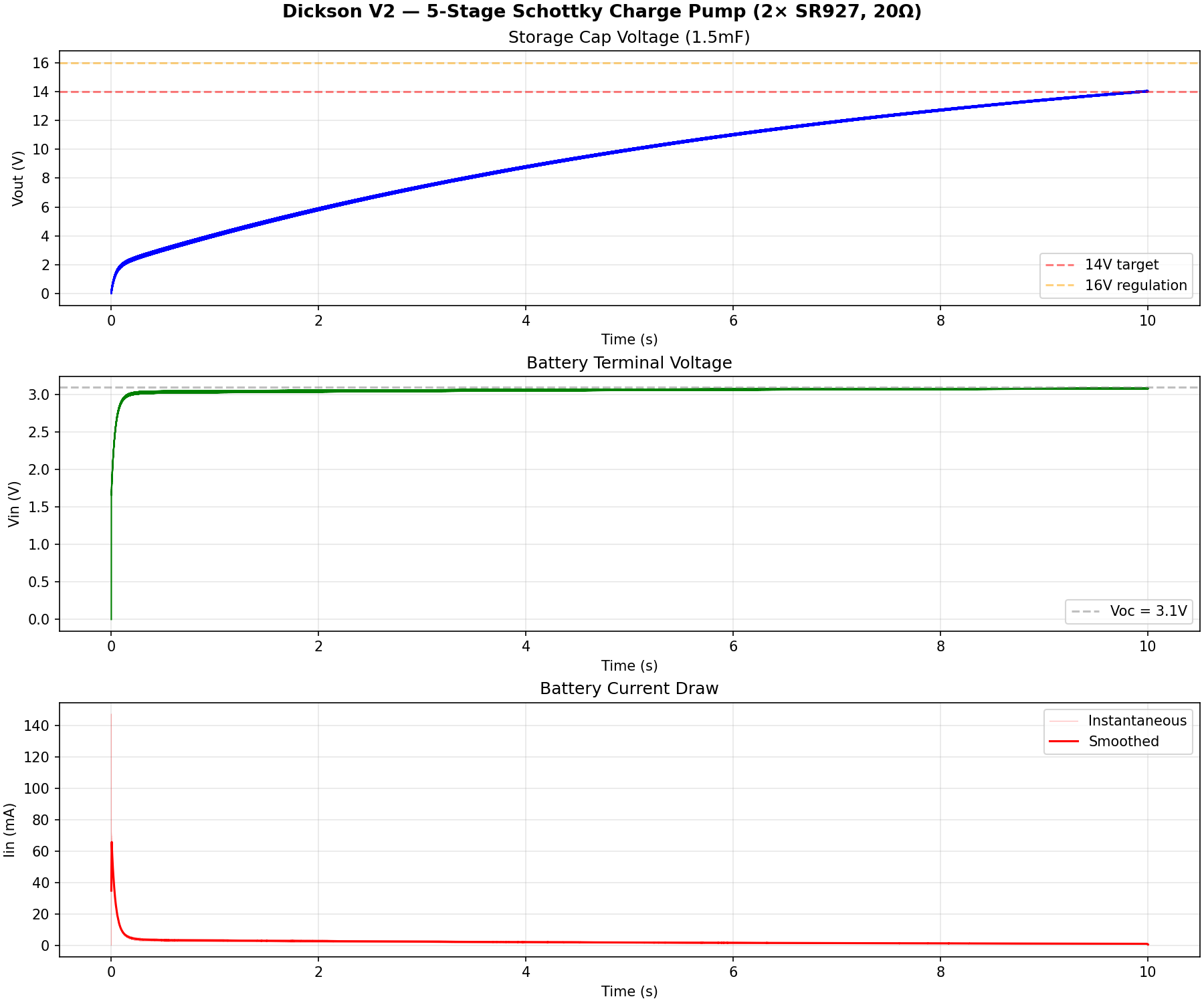
Simulation waveforms — output voltage charge-up and battery current over 30s
Note: Peak inrush current of 147.5 mA in the first few milliseconds
may require an NMOS inrush limiter. Quickly settles to <3 mA average.
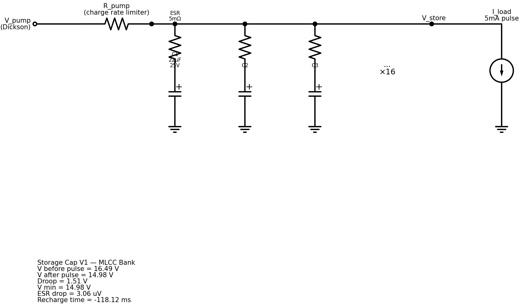
Storage Capacitor
MLCC Bank — Energy Storage
Stores energy between Dickson pump cycles to supply current pulses.
MLCC selected for zero leakage (critical for 54 mAh battery) and safe open-circuit failure mode.
X5R ceramic derated ~50% at 16V DC bias.
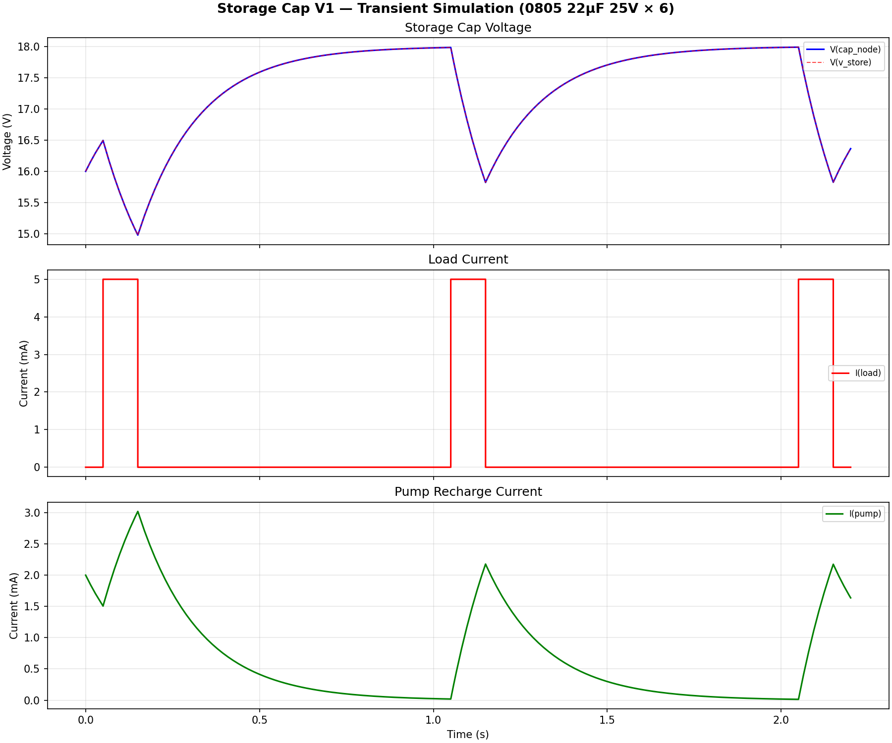
Testbench — pulsed current load with Dickson recharge model
Technology
Murata GRM21BR61E226ME44L — 22µF 25V X5R 0805
Bank configuration
24 caps — 3 rows × 8/side, 7mm board
Nominal capacitance
528 µF — effective ~264µF at 16V DC bias
Bank ESR
0.21 mΩ
Pre-pulse voltage
16.49 V
Post-pulse voltage
14.98 V — 5mA × 100ms worst case
Voltage droop
1.51 V — stays above 14V compliance
Recharge time
~118 ms — adequate for 1Hz repetition
Pulse response — voltage droop and recovery at 5mA, 1Hz
Alternative under evaluation: Panasonic EEH-ZK1E101UP polymer hybrid (100 µF, no DC bias derating,
6.3mm can) may be preferable — delivers full rated capacitance at 16V with only ~50 µA leakage
trade-off (11% of daily battery budget).
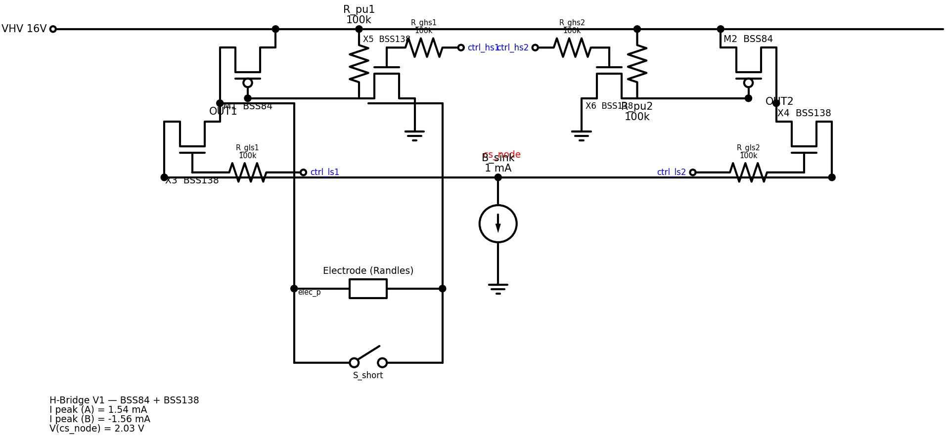
H-Bridge
Discrete Complementary MOSFET
BSS84 (PMOS high-side) + BSS138 (NMOS low-side) provide biphasic switching
with zero quiescent current. BSS138 level shifters drive the PMOS gates from 3.1V MCU logic.
Electrode shorting for passive charge balancing between phases.
Circuit schematic — complementary MOSFET H-bridge with level shifters and electrode shorting
Note: Minor charge injection from ideal gate drive coupling visible in simulation.
Will not occur in practice — MCU GPIOs have finite slew rate.
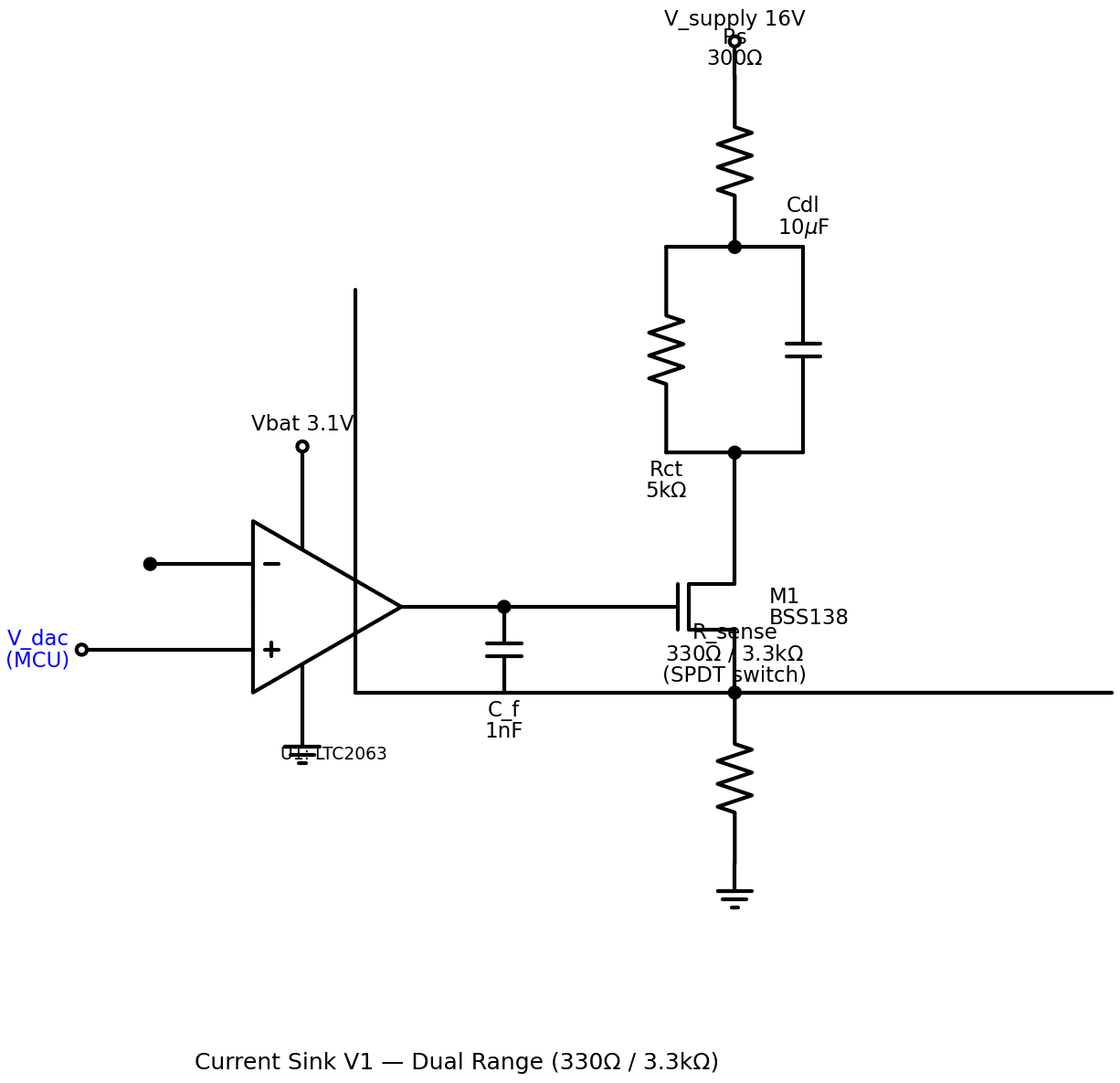
Current Sink
LTC2063 + BSS138 + Dual-Range Sense Resistor
Zero-drift op-amp feedback topology: Iout = Vdac / Rsense,
load-independent. Dual-range sense resistor (330 Ω / 3.3 kΩ) via SPDT analog switch
covers the full 10 µA–5 mA range with adequate DAC resolution.
1 nF Miller compensation optimises settling.
Circuit schematic — LTC2063 op-amp, BSS138 NMOS, TS5A3159 range switch
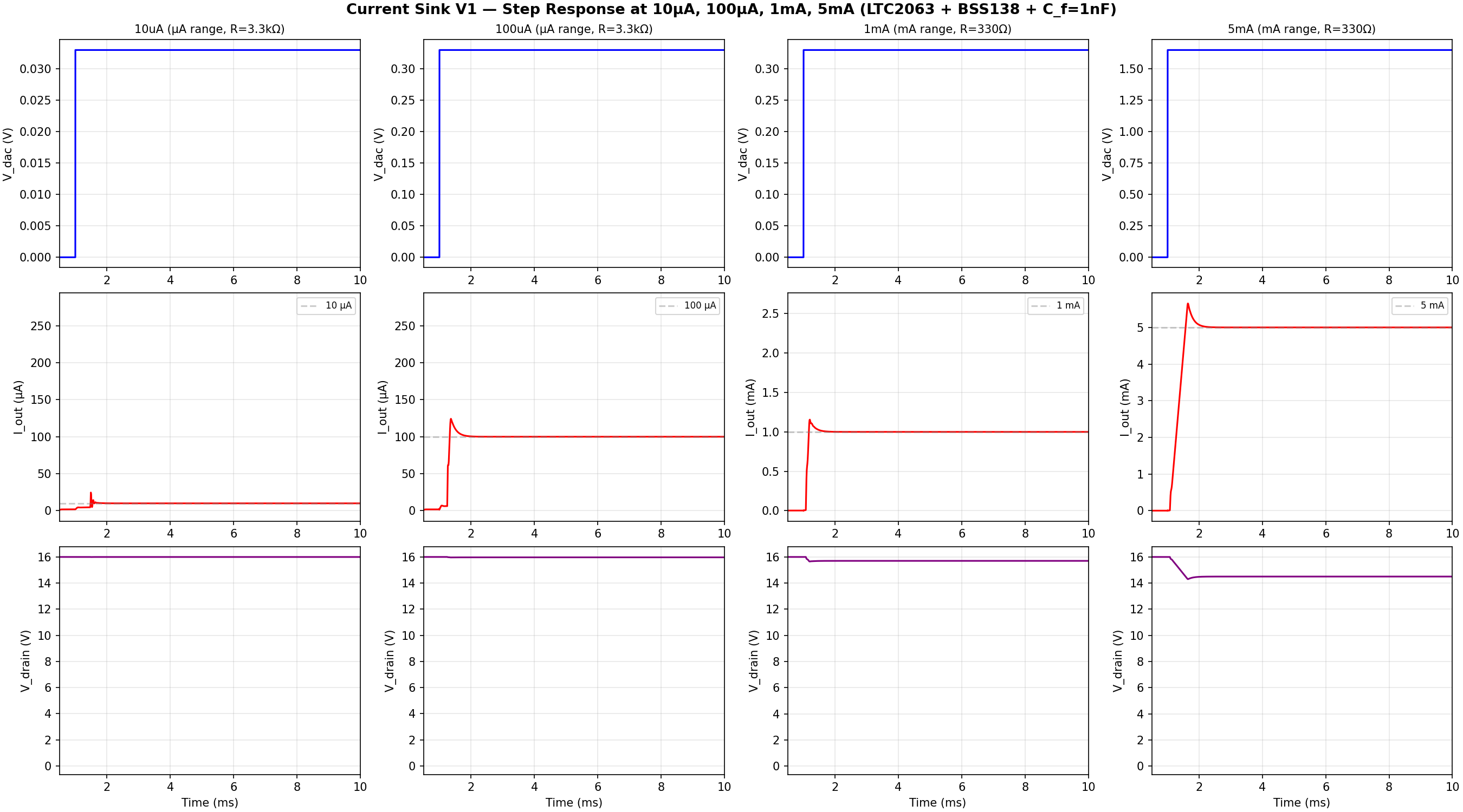
Step response — dual-range compensated, 10µA to 5mA test points
MCU
STM32L052T6 — Behavioral Model
Cortex-M0+ in WLCSP-36 (2.61 × 2.88 mm). Integrated 12-bit DAC eliminates
external IC. Ultra-low power: 0.27 µA standby. The behavioural LTSpice model
defines the firmware/hardware interface contract.
Pump clock
PA0 — TIM2_CH1 PWM — 10kHz, firmware-configurable
DAC output
PA4 — 12-bit, 0–3.1V — sets current sink amplitude
H-bridge control
PA8, PA9, PA10, PA11 — 4 GPIOs for HS/LS switching
Electrode short
PB4 — GPIO — charge balancing between phases
Range select
PB5 — GPIO — µA / mA sense resistor switch
ADC feedback
PB0, PB1 — pump Vout and current sense
Spare pins
19 — available for future features
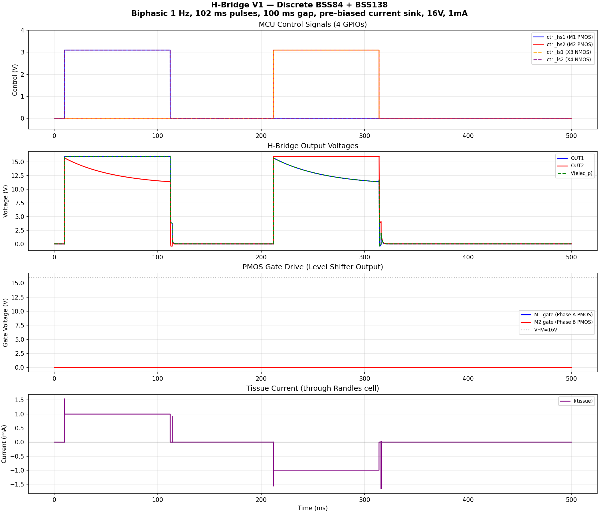
Stimulation Sequence (1Hz biphasic)
0–8ms: electrode shorted, current sink pre-biased →
10–112ms: Phase A (cathodic) →
114–210ms: interphase gap, electrode shorted →
212–314ms: Phase B (anodic) →
316ms+: idle until next cycle.
Dead times of 2ms between all transitions prevent overlap.
Summary
Compliance voltage
14.98 V min — after 5mA worst-case pulse (>14V spec)
Charge balance
0.16 nC net DC — vs <100nC spec
Current range
10 µA – 5 mA — all points settle <2ms
Quiescent draw
~2.3 µA — MCU standby + LTC2063 only
Pump charge time
9.87 s to 14V — one-time startup
Recharge between pulses
~118 ms — within 1Hz budget
All key requirements are met in simulation. The architecture is ready to proceed
to component selection and high-resolution simulation with full vendor models.