Phase 3 — PCB Layout
Development board PCB designed in KiCad with hand-solderable components. Schematic and component placement complete — ready for student review and routing.
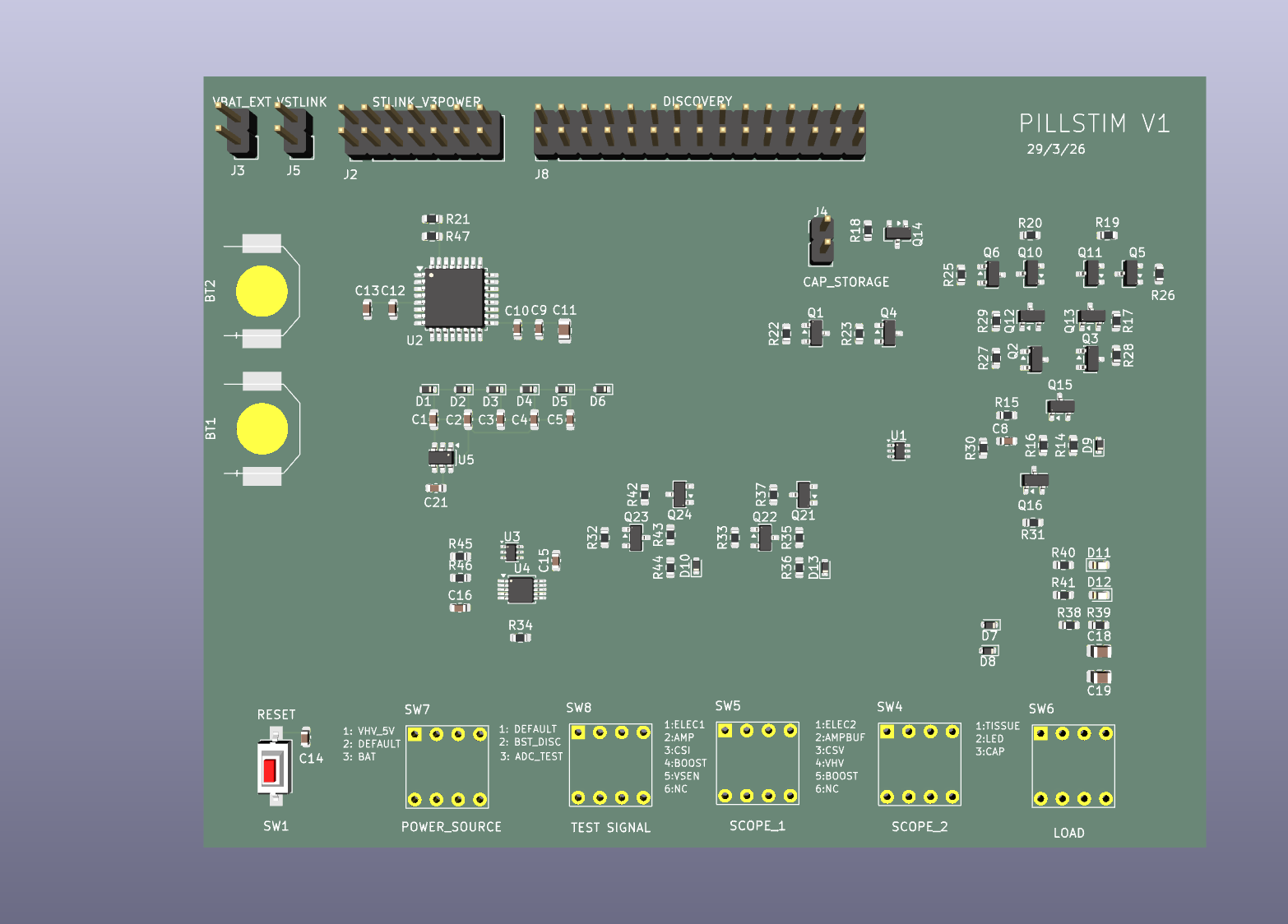
Overview
This is a development board designed to characterise and test the PillStim stimulation circuit. It replicates the pill electronics with hand-solderable components, and adds a debug harness that greatly improves testing speed and data collection. The board is designed around three external connections — an STLINK-V3PWR, a Digilent Analog Discovery 3, and an external storage capacitor — which together provide everything needed to fully test the circuit.
Inputs
| STLINK-V3PWR |
14-pin header (J2) + power terminals to VSTLINK (J5)
SWD debug, UART data, and regulated power supply to the board — all from a single instrument |
| Analog Discovery 3 |
30-pin IDE header (J8)
16 digital channels observe all MCU I/O. Waveform generator provides test signal injection (e.g. external boost clock). Two scope inputs are routed through front-panel selectors to any test point. |
| Storage capacitor |
External header (J4)
External capacitor allows easy swapping of values during characterisation without rework |
| Batteries |
2× SR927 coin cells (BT1, BT2) or external source via JST (J3)
Used in battery mode — not required during debug, where the STLINK provides power |
Outputs
| Electrodes |
Biphasic current stimulation output
The primary output of the PillStim circuit — drives the selected load (tissue model, LED, or capacitor) |
| AD3 scope channels |
Two analog outputs routed via front-panel selectors (SW4, SW5)
Any combination of test points can be observed without re-wiring. Electrode 1 and 2 are on separate selectors to allow differential measurement across the load. |
| AD3 digital channels |
All MCU I/O visible on the AD3 logic analyser
H-bridge timing, pump clock, DAC output, range select — captured in the same time base as the analog channels |
| UART |
Serial data via STLINK-V3PWR
Firmware telemetry, ADC readings, and diagnostics streamed to the host |
| LED indicators |
D11, D12
Quick visual confirmation that anodic and cathodic phases are firing — available when load selector is set to LED |
User Interface
Five rotary switches along the bottom edge configure the board for different test
scenarios. No re-wiring required between tests.
| Scope 1 (SW5) |
ELEC1, AMP, CSI, BOOST, VSEN, NC
Select which signal is routed to AD3 scope channel 1 |
| Scope 2 (SW4) |
ELEC2, AMPBUF, CSV, VHV, BOOST, NC
Select which signal is routed to AD3 scope channel 2. Electrode 1 and 2 are on separate selectors to enable differential measurement across the tissue load. |
| Load (SW6) |
Tissue — Randles cell model for realistic testing and shorting verification
LED — quick visual debug to confirm anodic and cathodic phases are working Cap — capacitive load to observe current waveform |
| Power Source (SW7) |
VHV_5V — bypass mode, powers H-bridge from AD3 +5V supply (bypasses boost)
Default — debug mode, circuit fully powered by STLINK-V3PWR BAT — battery mode, powered by button cells or external source via J3 |
| Test Signal (SW8) |
Default — normal operation
BST_DISC — boost circuit clocked by AD3 waveform generator ADC_TEST — ADC test mode |
| Reset (SW1) |
MCU hardware reset
Tactile pushbutton, active low |